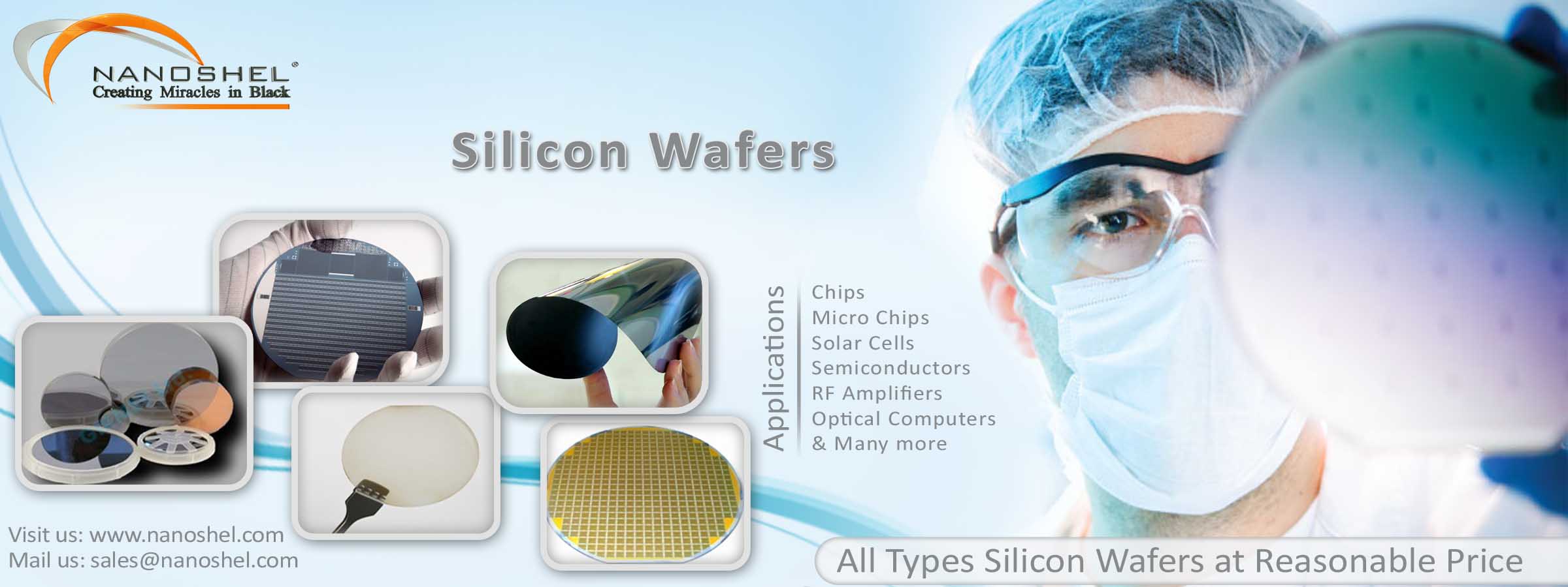
Phosphorus doped Silicon Wafers
Si, Dia: 8”, N Type
Stock No.
NS6130-10-1080
CAS
7440-21-3
MSDS

Specifications
COA
Catalogue
Phosphorus doped Silicon Wafers


Phosphorus doped Silicon Wafers
| Product | Phosphorus doped Silicon Wafers | |
| Stock No | NS6130-10-1080 | |
| CAS | 7440-21-3 | Confirm |
| Diameter | 8” | Confirm |
| Thickness | 500µm | Confirm |
| Crystal Orientation | <100> | Confirm |
| Type | N Type | Confirm |
| Growth Method | CZ | Confirm |
| Resistivity | 1-10Ω/cm | Confirm |
| CZ Resistivity | 1 to 150mΩ.cm | Confirm |
| TTV | <10µm | Confirm |
| STIR | <2µm | Confirm |
| GLOBAL TIR | <5µm | Confirm |
| LPD | <30 counts @ particles size>0.3µm | Confirm |
| Laser Mark | None | Confirm |
| Edge Profile | Rounded | Confirm |
| Doping | Phosphorous | Confirm |
| Bow | <5µm | Confirm |
| Standard Tolerance | ±0.5° | Confirm |
| Front Side Surface | Polished | Confirm |
| Backside Side Surface | Etched | Confirm |
| Quality Control | Each Lot of was tested successfully | |
| Main Inspect Verifier | Manager QC | |
Expert Reviews
Phosphorus doped Silicon Wafers
Contact Us
From us, you can easily purchase Phosphorus doped Silicon Wafers - (Si, Dia: 8”, N Type) at great prices. Place an online order and we will dispatch your order through DHL, FedEx, UPS. You can also request a quote by mailing us at sales@nanoshel.com. We invite you to contact us for further information about our company and our capabilities. At Nanoshel, we look forward to your suggestions and feedback.
Email Us:
sales@nanoshel.comcmg@nanoshel.com
🔆
Follow Us:
Direct Call Us:


USA – Sales/Research
+1 646 470 4911
+1 646 470 4911

UK – Sales/Research
+44 1782 454 144
+44 1782 454 144

Ireland – Sales/Research
+354 71 985 3714
+354 71 985 3714

India – Sales/Research
+91-9779550077
+91-9779238252
+91-9779550077
+91-9779238252
Note:
*Exchanges of materials/products are not permitted. Nanoshel does not offer refunds.
*US Dollar Cheques Not Accepted, Only Bank TT/Credit Cards Accepted
*Exchanges of materials/products are not permitted. Nanoshel does not offer refunds.
*US Dollar Cheques Not Accepted, Only Bank TT/Credit Cards Accepted