Yttrium Oxide Sputtering Target
Y2O3, Purity: 99.99%, Dia: 50.8mm
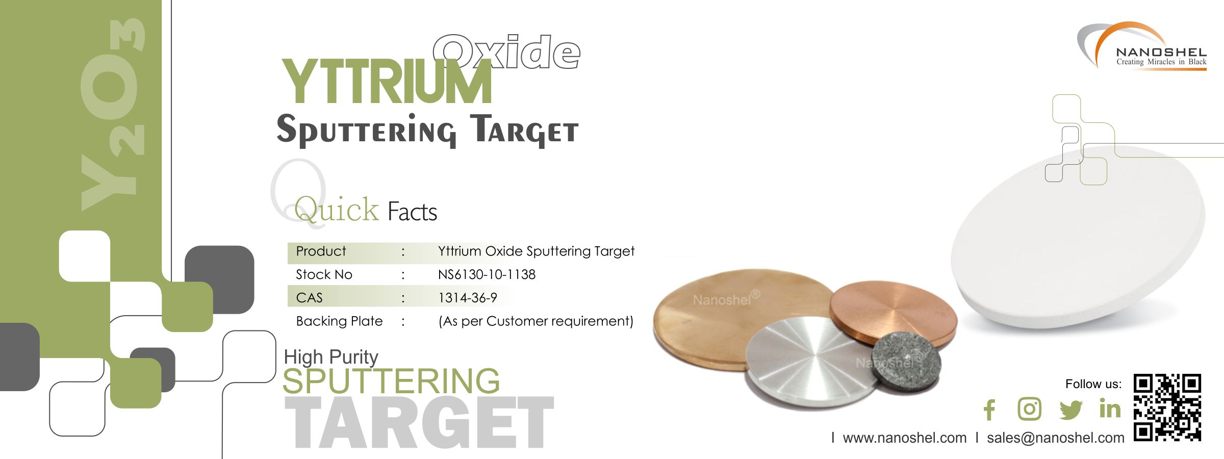
Stock No.
NS6130-10-1138
CAS
1314-36-9
MSDS

Specifications
COA
Catalogue

Yttrium Oxide Sputtering Target
Available Pack Size: 1Pc, 2Pcs, 5Pcs, 10Pcs & Bulk orders


Yttrium Oxide Sputtering Target
| Product | Yttrium Oxide Sputtering Target | |
| Stock No | NS6130-10-1138 | |
| CAS | 1314-36-9 | Confirm |
| Purity | 99.99% | Confirm |
| Diameter | 50.8 mm ± 1mm | Confirm |
| Thickness | 3 mm ± 0.5mm | Confirm |
| Molecular Weight | 225.81 g/mol | Confirm |
| Density | 5.010 g/cm³ | Confirm |
| Melting Point | 2425 °C | Confirm |
| Loss on ignition | 1.00 % | Confirm |
| Shape | Round | Confirm |
| Backing Plate | Copper (as per customer requirement) | |
| Size and Shape | Targets Diameter and thickness can be according to Customer Requirement | |
| Conclusion | The specifications Confirm with enterprise standard | |
| Quality Control | Each Lot of was tested successfully | |
| Main Inspect Verifier | Manager QC | |
Expert Reviews
Yttrium Oxide Sputtering Target
Contact Us
From us, you can easily purchase Yttrium Oxide Sputtering Target - (Y2O3, Purity: 99.99%, Dia: 50.8mm) at great prices. Place an online order and we will dispatch your order through DHL, FedEx, UPS. You can also request a quote by mailing us at sales@nanoshel.com. We invite you to contact us for further information about our company and our capabilities. At Nanoshel, we look forward to your suggestions and feedback.
Email Us:
sales@nanoshel.comcmg@nanoshel.com
🔆
Follow Us:
Direct Call Us:


USA – Sales/Research
+1 646 470 4911
+1 646 470 4911

UK – Sales/Research
+44 1782 454 144
+44 1782 454 144

Ireland – Sales/Research
+354 71 985 3714
+354 71 985 3714

India – Sales/Research
+91-9779550077
+91-9779238252
+91-9779550077
+91-9779238252
Note:
*Exchanges of materials/products are not permitted. Nanoshel does not offer refunds.
*US Dollar Cheques Not Accepted, Only Bank TT/Credit Cards Accepted
*Exchanges of materials/products are not permitted. Nanoshel does not offer refunds.
*US Dollar Cheques Not Accepted, Only Bank TT/Credit Cards Accepted